- 您现在的位置:买卖IC网 > Sheet目录17351 > AS1329B EB (ams)BOARD EVAL AS1329B
AS1329
Datasheet - A p p l i c a t i o n I n f o r m a t i o n
9.4 PCB Layout Guidelines
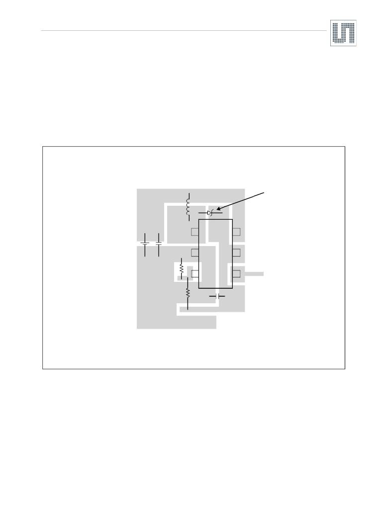
The high-speed operation of the AS1329 requires proper layout for optimum performance. Figure 29 shows the recommended component
layout.
A large ground pin copper area will help to lower the device temperature.
A multi-layer board with a separate ground plane is recommended.
Traces carrying large currents should be direct.
Trace area at pin FB should be as small as is practical.
The lead-length to the battery should be as short as is practical.
Figure 29. Recommended Single-Layer Component Placement
Optional
V IN
1 SW
AS1329
V IN 6
R 2
2 GND
V OUT
5
C IN
SHDNN
R 1
3
FB
SHDNN 4
C OUT
V OUT
www.ams.com/DC-DC_Step-Up/AS1329
Revision 1.12
16 - 20
发布紧急采购,3分钟左右您将得到回复。
相关PDF资料
SJA7501-1-1/2-50-WHITE
LOOP WHITE 1 1/2" X 50YD 0.12"
ECM08DRYH
CONN EDGECARD 16POS DIP .156 SLD
CS51411EVB
EVAL BOARD FOR CS51411 HI FREQ
RBM06DCWD
CONN EDGECARD 12POS DIP .156 SLD
A9BAG-1604F
FLEX CABLE - AFF16G/AF16/AFE16T
TARQ224K035
CAP TANT 0.22UF 35V 10% AXIAL
A9BAA-0502E
FLEX CABLE - AFJ05A/AE05/AFH05T
AS1329A EB
BOARD EVAL AS1329A
相关代理商/技术参数
AS1329BBTTT
制造商:AMS 功能描述:IC STEP-UP DC/DC CONVERTER 6-SOT-23 制造商:AMS 功能描述:IC, STEP-UP DC/DC CONVERTER, 6-SOT-23; Primary Input Voltage:1.2V; No. of Outputs:1; Output Voltage:5V; Output Current:220mA; No. of Pins:6; Operating Temperature Min:-40C; Operating Temperature Max:85C; Output Current Max:315mA ;RoHS Compliant: Yes
AS1329B-BTTT
功能描述:IC REG BOOST SYNC ADJ TSOT23-6 RoHS:是 类别:集成电路 (IC) >> PMIC - 稳压器 - DC DC 开关稳压器 系列:- 标准包装:50 系列:- 类型:升压(升压) 输出类型:可调式 输出数:1 输出电压:5 V ~ 25 V 输入电压:2.3 V ~ 5.5 V PWM 型:电流模式 频率 - 开关:600kHz,1.2MHz 电流 - 输出:1A 同步整流器:无 工作温度:-40°C ~ 85°C 安装类型:表面贴装 封装/外壳:8-TSSOP,8-MSOP(0.118",3.00mm 宽) 包装:管件 供应商设备封装:8-MSOP
AS1329B-EB
制造商:ams 功能描述:AS1329B Evaluation Board
AS1329B-TT_EK_ST
功能描述:AS1329B - DC/DC, Step Up 1, Non-Isolated Outputs Evaluation Board 制造商:ams 系列:- 零件状态:有效 主要用途:DC/DC,步升 输出和类型:1,非隔离 功率 - 输出:- 电压 - 输出:3.3V 或 5V 电流 - 输出:570mA 电压 - 输入:0.85 V ~ 5 V 稳压器拓扑:升压 频率 - 开关:1.2MHz 板类型:完全填充 所含物品:板 使用的 IC/零件:AS1329B 标准包装:1
AS1329C
制造商:AMSCO 制造商全称:austriamicrosystems AG 功能描述:Low Voltage, Micropower, DC-DC Step-Up Converters
AS1329C EB
功能描述:BOARD EVAL AS1329C RoHS:否 类别:编程器,开发系统 >> 评估板 - DC/DC 与 AC/DC(离线)SMPS 系列:- 产品培训模块:Obsolescence Mitigation Program 标准包装:1 系列:True Shutdown™ 主要目的:DC/DC,步升 输出及类型:1,非隔离 功率 - 输出:- 输出电压:- 电流 - 输出:1A 输入电压:2.5 V ~ 5.5 V 稳压器拓扑结构:升压 频率 - 开关:3MHz 板类型:完全填充 已供物品:板 已用 IC / 零件:MAX8969
AS1329CBTTT
制造商:AMS 功能描述:IC STEP-UP DC/DC CONVERTER 6-SOT-23
AS1329C-BTTT
功能描述:IC REG BOOST SYNC ADJ TSOT23-6 RoHS:是 类别:集成电路 (IC) >> PMIC - 稳压器 - DC DC 开关稳压器 系列:- 标准包装:1,000 系列:- 类型:降压(降压) 输出类型:可调式 输出数:1 输出电压:0.6 V ~ 4.5 V 输入电压:3 V ~ 5.5 V PWM 型:电流模式 频率 - 开关:3MHz 电流 - 输出:1.5A 同步整流器:无 工作温度:-40°C ~ 125°C 安装类型:表面贴装 封装/外壳:6-WDFN 裸露焊盘 包装:带卷 (TR) 供应商设备封装:6-LLP-EP(3x3) 产品目录页面:1300 (CN2011-ZH PDF) 其它名称:LM2831ZSDLM2831ZSDTR
